
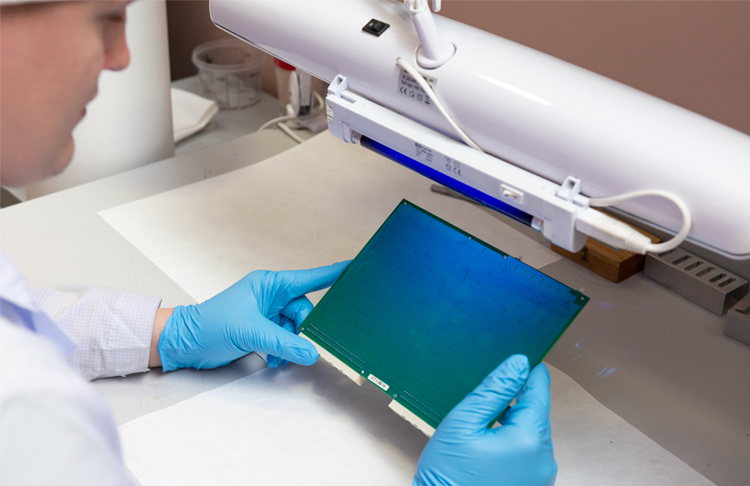
A leading semiconductor manufacturing company wanted to improve their defect identification process. Their existing system was not only tedious and time-consuming but also inefficient to deliver the expected results. This further led to poor yield analysis and production planning thereby affecting the company’s revenue margins. Therefore, they were looking for a high-speed and high-precision defect detection system.
“Improving semiconductor manufacturing yields up to 30%, reducing scrap rates, and optimizing fab operations is achievable with machine learning.” – Forbes
Softweb Solutions provided them with a backend tool for defect detection using deep learning. Our image analysis system differentiates between the defected and non-defected images of semiconductor wafers. The automated system helps the client to save both time and resources while achieving high levels of accuracy. Moreover, by collecting this defected and non-defected image data, the client is able to gain insights about the frequency and types of defects which can further be put in use to improve the overall production process.
Key features:
- Automated image classification
- Accurate defect detection using deep learning
- Defect identification in real-time
- Dashboard to analyze the type of defects